A guide to the latest trends in chip manufacturing
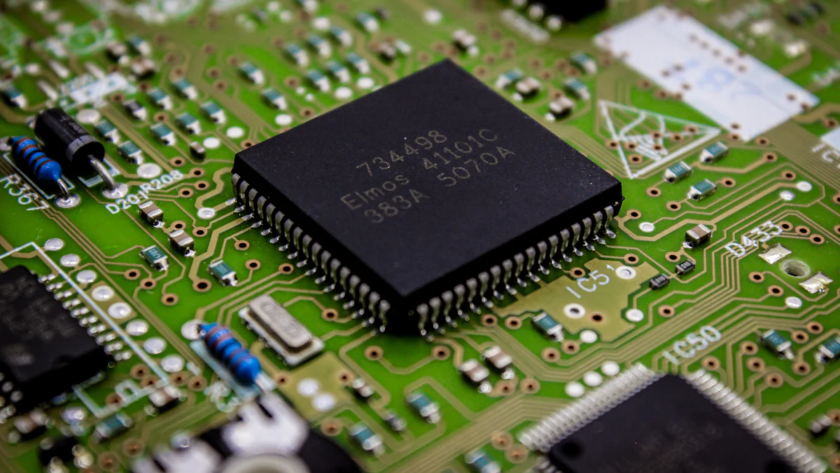
Chip manufacturing plays a crucial role in modern technology. The semiconductor industry is predicted to see an 18 percent annual increase by 2024, highlighting the rapid advancements and innovations in the field. IBM Research unveiled the world’s first 2 nm node chip in 2021, showcasing the continuous evolution of chip nodes. Staying updated with the latest trends in chip manufacturing is essential for leveraging new technologies and maintaining competitive advantage.
Advances in Chip Manufacturing
Smaller Node Sizes
Benefits of Smaller Nodes
Smaller node sizes in chip manufacturing offer several benefits. The primary advantage includes increased transistor density, which allows for more powerful and efficient chips. Higher transistor density leads to faster processing speeds and improved performance. Additionally, smaller nodes reduce power consumption, making chips ideal for mobile and IoT devices. The reduction in size also enables the production of compact and lightweight electronic devices.
Challenges in Manufacturing
Despite the benefits, smaller node sizes present significant challenges in chip manufacturing. As nodes shrink, maintaining performance and yield becomes increasingly difficult. The cost per die rises significantly, impacting overall production costs. Manufacturers face issues related to lithography, as creating smaller features requires advanced techniques like Extreme Ultraviolet (EUV) lithography. The complexity of ensuring optimal performance while reducing node size can degrade performance and increase prices.
3D Chip Stacking
Advantages of 3D Stacking
3D chip stacking represents a major advancement in chip manufacturing. This technique involves stacking multiple layers of chips vertically, which enhances processing power and speed. The vertical integration reduces the distance data needs to travel, resulting in lower latency and improved data transfer speeds. 3D stacking also optimizes space efficiency, making it suitable for compact devices. By integrating different functionalities into a single package, 3D stacking offers a versatile solution for advanced applications.
Current Applications
Current applications of 3D chip stacking span various industries. High-performance computing systems benefit from the increased processing power and speed. Mobile devices utilize 3D stacked chips to achieve better performance in a smaller form factor. Data centers leverage this technology to enhance server efficiency and reduce energy consumption. The automotive industry employs 3D stacking for advanced driver-assistance systems (ADAS) and autonomous driving technologies.
Chiplet Architectures
Modular Design Benefits
Chiplet architectures introduce a modular approach to chip manufacturing. This design allows for the integration of smaller, specialized chips called chiplets into a single package. The modular design offers several benefits, including flexibility in combining different functionalities. Manufacturers can mix and match chiplets to create customized solutions tailored to specific applications. This approach also simplifies the manufacturing process, as individual chiplets can be produced separately and then assembled.
Industry Adoption
The semiconductor industry has started adopting chiplet architectures due to their numerous advantages. Leading companies like AMD and Intel have integrated chiplet designs into their latest processors. This adoption allows for better scalability and performance optimization. The modular nature of chiplets facilitates easier upgrades and enhancements. As the demand for specialized and high-performance chips grows, chiplet architectures will likely become more prevalent in various sectors, including computing, telecommunications, and automotive.
Innovations in Manufacturing Processes
Extreme Ultraviolet Lithography (EUV)
How EUV Works
Extreme Ultraviolet Lithography (EUV) represents a significant leap in chip manufacturing technology. EUV uses light with a wavelength of 13.5 nanometers to create extremely small features on semiconductor wafers. This method allows for the production of chips with higher transistor densities. The process involves generating EUV light by heating tin droplets with a laser. Mirrors then focus and direct the light onto the wafer through a mask that defines the chip's pattern. This technique enables the creation of intricate and precise patterns essential for advanced semiconductor devices.
Impact on Production Efficiency
EUV lithography significantly impacts production efficiency in chip manufacturing. The ability to print smaller features means manufacturers can produce more powerful and efficient chips. For instance, EUV has enabled the mass production of logic chips at the 7nm technology generation, achieving tight pitches for metal lines. This advancement reduces the number of processing steps required, lowering production costs and increasing throughput. By pushing the limits of nanofabrication, EUV lithography enhances overall manufacturing efficiency and performance.
Advanced Packaging Techniques
System-in-Package (SiP)
System-in-Package (SiP) is an advanced packaging technique that integrates multiple integrated circuits (ICs) into a single package. SiP combines different functionalities, such as processors, memory, and sensors, into one compact module. This integration improves performance and reduces the space required for electronic components. SiP offers flexibility in design, allowing manufacturers to create customized solutions tailored to specific applications. The technique also simplifies the assembly process, leading to faster production times and lower costs.
Fan-Out Wafer-Level Packaging (FOWLP)
Fan-Out Wafer-Level Packaging (FOWLP) represents another innovative approach in chip packaging. FOWLP involves redistributing the input/output (I/O) connections of a chip across a larger area, creating a fan-out pattern. This method enhances thermal performance and electrical characteristics. FOWLP eliminates the need for traditional substrates, reducing the overall package size and improving signal integrity. The technique supports higher I/O densities, making it ideal for applications requiring high performance and miniaturization, such as mobile devices and wearable technology.
Automation and AI in Chip Manufacturing
Role of AI in Quality Control
Artificial Intelligence (AI) plays a crucial role in quality control within chip manufacturing. AI-powered inspection systems analyze vast amounts of data to detect defects at microscopic levels. These systems use machine learning algorithms to identify patterns and anomalies that human inspectors might miss. By ensuring higher accuracy and consistency, AI enhances the overall quality of semiconductor products. Predictive maintenance powered by AI also helps in anticipating equipment failures, reducing downtime, and improving yield rates.
Automation in Production Lines
Automation transforms production lines in chip manufacturing. Automated systems handle repetitive and complex tasks with precision and speed. Robots and automated machinery perform wafer handling, lithography, etching, and packaging processes. Automation reduces human error, increases production efficiency, and lowers labor costs. The integration of AI with automation further optimizes manufacturing processes. AI algorithms analyze real-time data to adjust parameters and improve process control. This synergy between AI and automation leads to higher productivity and better-quality semiconductor devices.
Materials and Sustainability

New Semiconductor Materials
Gallium Nitride (GaN)
Gallium Nitride (GaN) has emerged as a significant material in semiconductor manufacturing. GaN offers superior efficiency compared to traditional silicon-based materials. This efficiency stems from GaN's wide-bandgap properties, which allow for higher voltage operation and faster switching speeds. These characteristics make GaN ideal for power electronics, RF components, and LED technology. GaN devices exhibit lower conduction and switching losses, enhancing overall performance and energy savings.
Silicon Carbide (SiC)
Silicon Carbide (SiC) is another advanced material gaining traction in the semiconductor industry. SiC's wide-bandgap properties enable high-temperature operation and high-voltage capabilities. These features make SiC suitable for applications in electric vehicles, renewable energy systems, and industrial power supplies. SiC devices demonstrate reduced thermal resistance, leading to improved heat dissipation and reliability. The adoption of SiC in power electronics contributes to higher efficiency and smaller system sizes.
Eco-Friendly Manufacturing Practices
Reducing Carbon Footprint
Reducing the carbon footprint in chip manufacturing has become a priority. Manufacturers implement energy-efficient processes to minimize environmental impact. Utilizing renewable energy sources for production facilities helps lower greenhouse gas emissions. Companies also invest in advanced technologies to optimize energy consumption during manufacturing. By adopting these practices, the semiconductor industry aims to achieve more sustainable production methods.
Recycling and Waste Management
Recycling and waste management play crucial roles in eco-friendly manufacturing. Semiconductor companies focus on recycling materials used in the production process. This includes reclaiming silicon wafers, metals, and chemicals. Effective waste management strategies ensure the safe disposal of hazardous materials. Implementing these practices reduces the environmental footprint and promotes resource conservation. The industry continues to innovate in recycling techniques to enhance sustainability.
Energy Efficiency in Chips
Low-Power Design Techniques
Low-power design techniques are essential for creating energy-efficient chips. Engineers employ various methods to reduce power consumption in semiconductor devices. Techniques such as dynamic voltage scaling, clock gating, and power gating help minimize energy usage. These approaches optimize the performance-to-power ratio, making chips suitable for battery-operated devices. Low-power designs extend battery life and improve the overall efficiency of electronic products.
Impact on Battery Life and Performance
Energy-efficient chips significantly impact battery life and performance. Devices with low-power chips require less frequent charging, enhancing user experience. Improved battery life extends the operational time of mobile devices, wearables, and IoT gadgets. Additionally, energy-efficient chips contribute to better thermal management, preventing overheating and ensuring reliable performance. The focus on energy efficiency aligns with the growing demand for sustainable and high-performance electronic devices.
Keeping up with the latest trends in chip manufacturing remains crucial. These advancements shape future technology, driving innovation and efficiency. Staying informed about these trends ensures a competitive edge in the rapidly evolving semiconductor industry. Engaging with ongoing developments allows for leveraging new technologies effectively. The continuous evolution in chip manufacturing promises significant impacts on various sectors, enhancing performance and sustainability.
See Also
Insider Tips for Semiconductor Industry Quality Control
Mastering Manufacturing Success in 2024: Supply Chain Insights
Navigating Manufacturing Success: Essential Strategies
Unlocking High-Tech Manufacturing Success: Consulting Demystified
Collaborative Innovation: Strengthening High-Tech Manufacturing Partnerships